• Online Quote
  • Upload Gerber File
  • Payment
  • Fabrication
  • Delivery
  • Confirm and Review

Premium PCB Instant Quote

Our premium PCB service combines advanced process control systems with precision engineering capabilities. Designed for industries where reliability is crucial, our premium PCBs excel in automotive, medical, industrial, and other applications.

Basic Information

Base Material: param picture FR-4(Through Hole Board) param picture HDI(Buried/Blind Vias)
Layers:

The number of copper layers in the board.

2 4 6 8 10 12 14 16 18 20 22 24
HDI Order:

First-order: mainly includes single-sided or double-sided micro-hole processes, and the circuit layer has only one layer. This type of HDI PCB is suitable for applications with high requirements on cost and space, such as consumer electronics.

Second-order: contains two circuit layers, which are more complex but also more powerful than first-order HDI PCBs. They can handle higher signal frequencies and are suitable for applications that require high performance, such as high-end communication equipment and computer hardware.

Third-order: contains three circuit layers. They are the most complex type at present. They can handle the highest signal frequency and the maximum data transmission rate. They are usually used in applications that require the highest performance, such as aerospace and military equipment.

First-order Second-order Third-order
FR4-TG:

TG stands for Glass Transition Temperature.

The typical TG is 130℃ or higher, while medium TG is generally greater than 150℃, and advanced TG is typically above 170℃. The material's temperature resistance improves as the TG increases.

TG150(S1000H) TG170(S1000-2M)
Different Design:

Fill in how many different designs you have in your Gerber file, divided by V-cuts, stamp holes, or milled slots.

Example
Delivery Type:

The delivery type refers to the method by which you request CyberPCB to produce and deliver your PCB design.

Single PCB:  Your design will be produced and delivered as individual PCBs.

Panel by Customer:  You are responsible for constructing the PCB panel and providing us with the panelized data for production.

Panel by CyberPCB:  We will construct the panel for you, incorporating v-cuts based on your requirements. (Please note that we only offer panelizing services for PCBs with regular shapes such as rectangles and circles. For PCBs with irregular shapes, you will need to panelize them yourself.)

Single Piece Panel By Customer Panel By CyberPCB
Size:

The board size is determined by the customer and represents the length and width of the board. 

For circular boards, it corresponds to the diameter of the circle. 

In the case of boards with irregular shapes, the measurements are based on the maximum dimensions of the shape.

x
mm
inch'↔mm
Single Pcb Size
Quantity:

Quantity of single or panelized boards needed for the order.

sets
Panel Format:

 Please specify the number of columns/rows in the PCB panel array. For example:
Panel Format

Columns:
x
Rows:
Edge Rail:

Edge rails are located at the board edges to facilitate easier fixation of the boards onto a machine. The rails can be easily cut after assembly.

Route Process:

 The PCBs within the panel are interconnected as depicted in the following diagram:

None Panel as V-Scoring Panel as Tab-Route Both V-Scoring & Tab-Routing
X-out Panel:

 There is a possibility of defective PCBs within the panel.

If you choose not to accept the X-out in the panel, the cost will increase accordingly.

Accept Not Accept
Product Standard: IPC 6012 Class 2 IPC 6012 Class 3 IATF16949 ISO13485

Process Information

PCB Thickness:

 The board thickness represents the final thickness of the PCB after production, with an approximate error of 10% (+/-10% for T>=1mm or +/- 0.1mm for T<1mm). This error primarily stems from solder mask and copper sinking.

If you have specific thickness error requirements, kindly include them in the "Other Requirements" section.

PCB Thickness

0.4 0.6 0.8 1.0 1.2 1.6 2.0 2.4 2.8 3.0 3.2 3.6 4.0 4.4 4.8
Solder Mask:

The solder mask color refers to the color applied to the surface of the PCB.

Green and white are the available default colors for the solder mask. Selecting any other color will incur an additional fee.

Green White Yellow Blue Red Matt Black Black Purple Matt green param picture None
Silkscreen:

In most cases, the silkscreen is printed in white on the PCB. 

However, when using a white solder mask, the silkscreen is printed in black. 

It's important to note that the white silkscreen may appear less distinct on a gray surface. It is not recommended to have a silkscreen on the bare aluminum surface.

Silkscreen

White Black param picture None
Surface Finish:

 Surface finish plays a crucial role in PCB production as it serves multiple purposes. Firstly, it acts as a protective layer to prevent copper oxidation, which could render the PCB non-functional. Secondly, it provides a smooth surface that facilitates the soldering of components onto the PCB.

HASL (Hot Air Solder Leveling) is a cost-effective surface finishing option that involves the application of a thin protective layer of tin/lead on the PCB.

ENIG (Electroless Nickel Immersion Gold) has emerged as the industry's preferred surface finish due to its advantages, including a flat surface, lead-free and RoHS compliance, extended shelf life, and the ability to maintain tighter tolerances for plated holes.

OSP(Organic Solderability Preservatives) is also known as anti-tarnish. It involves the formation of an organic protective layer on clean and bare copper through adsorption.

ENEPIG (Electroless Nickel Electroless Palladium Immersion Gold) is a surface finish similar to ENIG (Electroless Nickel Immersion Gold) in that both processes involve the deposition of electroless nickel on top of copper plating. The key distinction is that while ENIG has gold directly deposited on top of the nickel layer, ENEPIG incorporates an additional layer of palladium between the nickel and final gold layer.
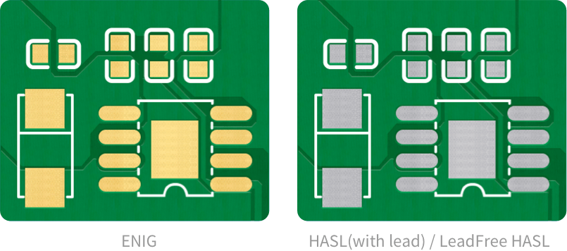
HASL Lead Free ENIG(Immersion Gold) OSP ENEPIG Hard Gold Immersion Silver(Ag) Immersion Tin HASL Lead Free + Selective Immersion Gold None(Plain Copper)
Thickness of Immersion Gold:

1U" 2U" 3U" 4U" 5U"
Thickness of ENEPIG: Ni:200U" Pd:2U" Au:2U" Ni:200U" Pd:3U" Au:3U" Ni:200U" Pd:4U" Au:4U"
Thickness Of Hard Gold:

Depth of hard gold plating on PCB surface.

Au:5U"/Ni:120U" Au:10U"/Ni:120U" Au:15U"/Ni:120U" Au:20U"/Ni:120U" Au:25U"/Ni:120U" Au:30U"/Ni:120U"
Thickness Of Immersion Gold:

Depth of gold coating on PCB surface.

1U" 2U" 3U"
Min Spacing:

 The minimum width of the copper trace and the minimum spacing between two traces.

Our engineers will verify the minimum spacing.

Min Spacing

3/3mil 4/4mil 5/5mil 6/6mil↑ 8/8mil↑ 10/10mil↑ 20/20mil↑
Min Hole Size:

 The minimum via diameter.

Our engineers will verify the minimum hole size.

Min Hole Size

0.15mm 0.2mm 0.25mm 0.3mm 0.4mm↑ 0.5mm↑ 0.6mm↑
Outer Copper:

The copper weight, measured in ounces per square foot, determines the thickness of copper on the outer layers of the PCB.

ps: 1oz=35um

1oz 2oz 3oz 4oz 5oz 6oz
Inner Copper:

The copper weight refers to the amount of copper on the inner layers of multilayer PCBs.

ps: 1oz=35um

0.5oz 1oz 1.5oz 2oz 3oz 4oz
Via Process:

Tented Vias Untented Vias Plugged Vias Resin Plug R-PTH
Contains BGA:

BGA stands for Ball Grid Array, which is a type of packaging used to connect integrated circuits and PCBs using surface mount technology.

No Yes
BGA Pads Spacing: >=0.4mm(16mil) <0.4mm(16mil)
Impedance Control:

To improve transmission speed, PCB conductors carry various signals. Impedance variations caused by factors like etching, layer thickness, and line width can distort the signals.

"Impedance control" ensures high-speed PCB conductors stay within a specific range. The typical tolerance is ±10%.

If impedance requirements are documented but not selected when placing the order, it will be considered as disregarding the impedance requirement.

No Yes
Impedance Control Report: No Yes
Gold Fingers:

 Gold fingers are the gold-plated contacts located along the connecting edges of PCBs. They are exclusively gold-plated when the ENIG surface finish is selected. However, if you choose the HASL surface finish, we will use HASL for the edge connector plating.

Gold Fingers

No Yes
Test method:

To detect open and short circuit issues, testing will be conducted on all PCBs. A test rack will be provided for batch orders.

Flying Probe Test Test Rack
Confirm Production File:

If you choose Yes, we'll email you the PCB production file, and production will proceed once you confirm. The lead time may be extended depending on the communication cycle.

No Yes

Advanced Options

Special Techniques: Edge Plating

 Edge plating on PCB enhances durability, EMC performance, grounding, edge protection, EMI reduction, signal integrity improvement, and reliable electrical connections.

Edge plating

Carbon Ink

Carbon ink is created by coating the PCB substrate with carbon-based conductive ink, which is then cured to form a carbon film conductive pattern. It offers several benefits, including low cost, excellent impedance control, high reliability, and strong corrosion resistance.

Countersink/Counterbore

The main difference between a countersink and a counterbore lies in the size and shape of the holes they create, as well as the screws or tools used.

A counterbore hole is deeper and has a square-like shape, providing a space for the screw head's shoulder to rest. This type of hole also allows for the use of washers if needed.

Countersink Counterbore

Peelable Soldermask

Peelable soldermask, also known as a peelable blue gel(pad), is primarily utilized for safeguarding the board's surface during production processes.

Press-fit Hole

Press-fit holes are specifically designed to accommodate components with press-fit pins. These pins are inserted into the holes and firmly pressed to establish a reliable and secure connection.

Press-Fit Holes

Chamfering

The connecting finger is similar to the connecting part between the RAM and the RAM slot, plated with thick gold. 
The edge of the board of the connecting part needs to be chamfered for dipping.

4-Wire Kelvin Test:

We highly recommend choosing this option for PCBs used in automotive, military, or aerospace applications that demand high precision and reliability.

4-wire Kelvin testing is a methodology that utilizes high-resolution measurements to accurately detect small resistance changes. These measurements typically fall within the milliohm range, whereas standard electrical test measurements are in the ohm range. To efficiently identify hidden defects like hole integrity, a 4-wire Kelvin test is necessary.

No Yes
Hole Copper Thickness:

Please choose the desired copper thickness for the holes you require.

Castellated Holes:

Castellations are plated through holes positioned along the edges of a printed circuit board. They are created by cutting through the board to form a series of half holes.

The minimum diameter for castellated holes is 0.60mm.

Castellated Holes

UL Marking:

To include UL marking on the board, please select the appropriate layer where you would like to add.

Board Outline Tolerance:

Regular and precision CNC routing methods primarily differ in the alignment process and the number of routing passes. 

In regular routing, the panel is secured at points outside individual PCBs, whereas precision routing utilizes alignment holes within each board for positioning. 

Regular routing involves a single-pass process, whereas precision routing consists of a rough pass followed by a fine pass.

For example, for a PCB with dimensions of 100mm x 80mm:

±0.2mm(Regular) ±0.1mm(Precision)
Test Reports:

Test reports included in the package.

Electric Test Quality Assurance Certificate Final Inspection Surface Plating Thickness Test Solderability Test Thermal Stress Test Microsection Measurement Ionic Contamination Test
Test Report Type: Electronic Paper
Paper Between PCBs:

CyberPCB offers a service of inserting paper strips between PCBs to prevent scratches and maintain the quality of shipments.

Especially for PCB with Black/Matte Black solder mask and Surface treatment of Immersion Gold/ Gold Plating.

Yes
Remove Product No.:

CyberPCB will include our product number on the PCB to differentiate your PCBs from others.

If you wish to have it removed, an additional charge of about $1.5 will apply.

If you prefer to have the product number placed in a specific location, please indicate the desired location by adding the text "CYBCYBCYB" in the silkscreen layer, the font size should be larger than 0.8mm in height and 5mil in width. There is no additional charge for this option.

Remove Product No.

No Yes Specify a Location
+Add PO No.:
Other Requests:
PCB Assembly Quote The PCBs above need assembly
SMD-Stencil Quote Order together with PCB
Border Type: Framework Non-framework Enlarge example image
Stencil Type:

1: Stencil for Solder Paste: Directly print solder paste on the pad, paste the SMD components, and reflow solder them together. The plug-in components are manually welded.

2: Stencil for Adhesives: First, print the adhesives, then add the components. After the components are firmly adhered to the PCB, place and wave solder the plug-in components together.

3: Step Down Stencil: Due to the different solder paste requirements for welding various components on the PCB, ordinary laser stencils can only control the amount of solder paste through the size of the openings.

Stencil for Solder Paste Stencil for Adhesives Step Down Stencil
Printing Method:

Fully automatic printing: Most fully automatic printed solder paste stencils use a half-quarter MARK point.
Manual Printing, Semi-automatic Printing: Solder paste stencils can be used without MARK points.

Semi-automatic Printing Fully Automatic Printing Manual Printing
Size(mm):

Please choose the size rules according to the PCB size (plate size) and the equipment used for the stencil.

If you have any questions about the size, contact your dedicated salesperson for confirmation.

Size(mm):

Please choose the size rules according to the PCB size (plate size) and the equipment used for the stencil.

If you have any questions about the size, contact your dedicated salesperson for confirmation.

Size(mm):

Please choose the size rules according to the PCB size (plate size) and the equipment used for the stencil.

If you have any questions about the size, contact your dedicated salesperson for confirmation.

Size(mm):

Please choose the size rules according to the PCB size (plate size) and the equipment used for the stencil.

If you have any questions about the size, contact your dedicated salesperson for confirmation.

Stencil Side:

Depending on how many sides of your PCB need to be soldered.

Top Bottom Top & Bottom (On a Single Stencil) Top & Bottom (On two Separate Stencils)
Quantity:
pcs
Thickness:

The stencil thickness is selected according to the component sizes.

0.08mm 0.10mm 0.12mm 0.15mm 0.2mm 0.25mm 0.3mm
Existing Fiducials:

Fiducial Marks

A fiducial mark is an alignment mark used for surface mount assembly machines.

In general, machine assembly requires fiducial marks. However, fiducial marks are not necessary when placing parts by hand.

None Half Lasered Mark Point Positioning PCB Drill Positioning
Electropolishing:

Electropolishing, also known as electrochemical surface treatment or electrochemical deburring, results in an optimized surface quality.

For PCB boards with IC pin spacing less than or equal to 0.4 mm or with BGA packages, it is strongly recommended that the steel mesh be electropolished.

No Yes
+Add PO No.:
Other Requests:
! You acknowledged that you have read and understand our content policy, and certify that your technical data and any related items are not (1) controlled under the ITAR, (2) subject to the EAR, or (3) weapons or any similar or related items or components thereof.
Pricing Information

Once all necessary parameters are provided, the price can be calculated.

Note:
1. Please note that we will provide a revised quotation based on the review of your documents, and the final price may be subject to change accordingly.
2. If your specific requirements are not listed in the "Online Quote" section, please specify them in the "Other Requests" box.